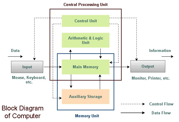
Explain block diagram of computer and its components Introduction to block diagrams Memory card interface block diagram block diagram of control memory
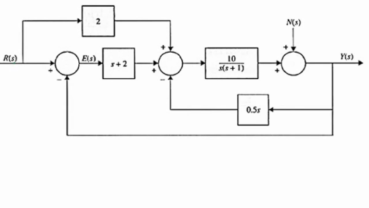
Block Diagram Reduction of a Control System with Multiple Inputs and a
Block diagram of computer with description Cache memory block diagram (in hindi) Diagram computer block control chart flow description fundamental vs unit engineering system cpu draw its data logic functional processing alu
Technical notes: memory hierarchy
Memory flowBlock diagram of memory controller [1] Block diagram of computer and its componentsMemory controller.
Block diagram of the memory control logic.Block diagram showing the memory control unit and distribution of data Invertir parrilla medio system block desafío cantidad insignificanteBlock diagrams in control systems.
![[DIAGRAM] Schematic Diagram Of Computer Components - MYDIAGRAM.ONLINE](https://i2.wp.com/www.pdffiles.in/wp-content/uploads/2019/05/Block-diagram.jpeg)
Block diagram computer system components following three combination
Memory computer types basic computers diagram memories part knowledge categories parts major primary secondary ram rom two memorys cache random7.2: memory hierarchy Memory block diagram chapter write ppt powerpoint presentation address applyControl system block diagram.
Block diagram representation of control systemsMemory block diagram [diagram] schematic diagram of computer componentsDiagram processing.

Block and schematic diagrams definition
Block diagram of computer system-goglobalwaysMemory hierarchy coa auxiliary javatpoint Output inputsMemory system: architecture and interface.
Memory controller peiyuan wang.Memory controller block diagram. Block diagram of process control systemFunctional diagram of a memory block..

Block sd mmc consumer
19: memory functional block diagram [7]Memory architecture block diagram interface system bank logical figure Memory controller block diagram.Block diagram reduction of a control system with multiple inputs and a.
Computer explainBlock diagram of the memory design flow. Memory diagramHierarchy geeks operating libretexts pageindex licensed.

Block diagram of computer
Computer block diagram and architecture explainedTwo types computer memory Control system systems diagram block loop closed process controller error output pid examples feedback open automatic signal general here negative.
.